-
Our latest Gallium Oxide results were presented at PhD student conference ELITECH’25
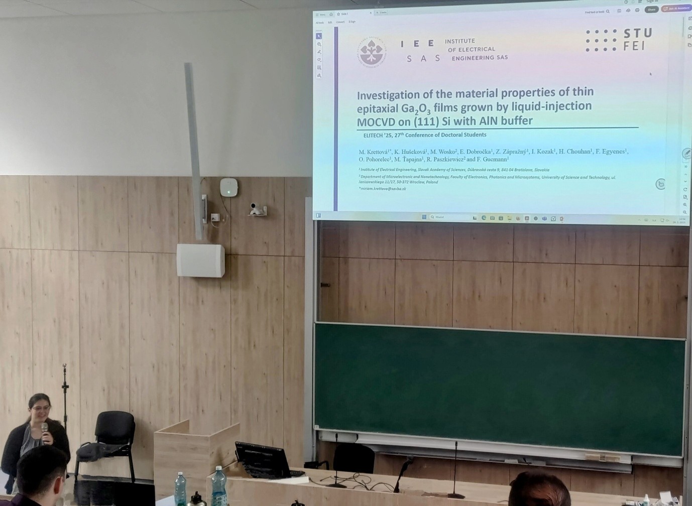
Our freshmen PhD students Ms Miriam Krettová, Mr Roshan Jeevan Chidambaram, and Mr Sai GuruKrishna Vadlamudi presented their latest results achieved within the CUBES project on growth of monoclinic gallium oxide, structural defects in its rhombohedral phase, and various aspects of homoepitaxial and heteroepitaxial power switching transistors at the 27th Conference of doctoral students ELITECH’25…
-
May exchange with the University of Žilina
Late May an interinstitutional exchange took place at IEE SAS. A delegation from University of Žilina led by Prof. Dušan Pudiš have visited us and presented the newly started collaboration on UV photonics based on Ga2O3. Mr Marek Zdurienčík also took part in the Ga2O3 growth and processing of Ga2O3 based photonic structures. We are…
-
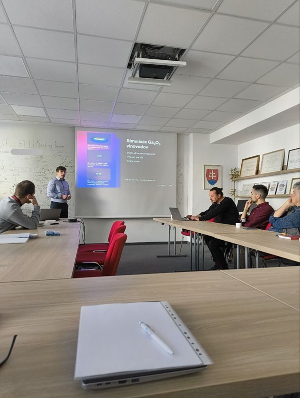
Workshop on (U)WBG semiconductor materials and devices
We organised a successful 2-day workshop on 28th and 29th April dedicated to (U)WBG semiconductor materials and devices in the Centre for Energy Research MFA (Budapest, HU). Delegates from all founding institutions – IEE SAS, Łukasiewicz IMiF, and the Centre for Energy Research, MFA, were attending the workshop. During the workshop, achieved competitive research results…
-
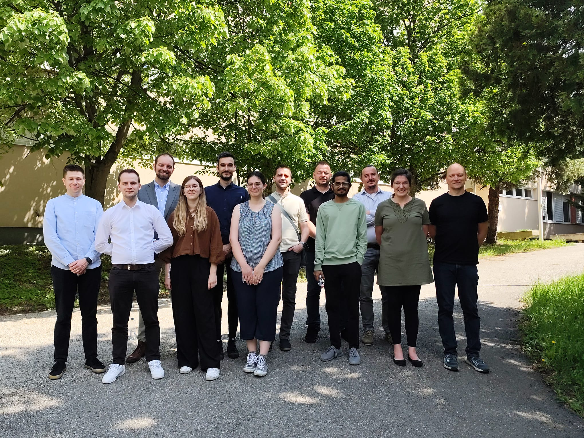
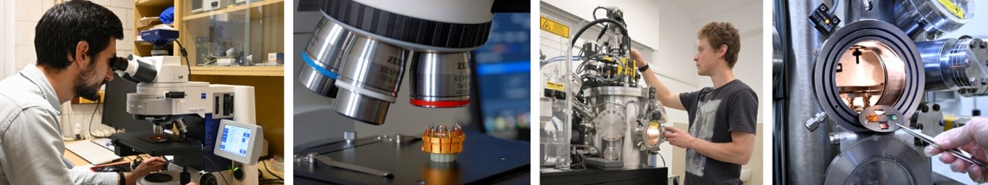
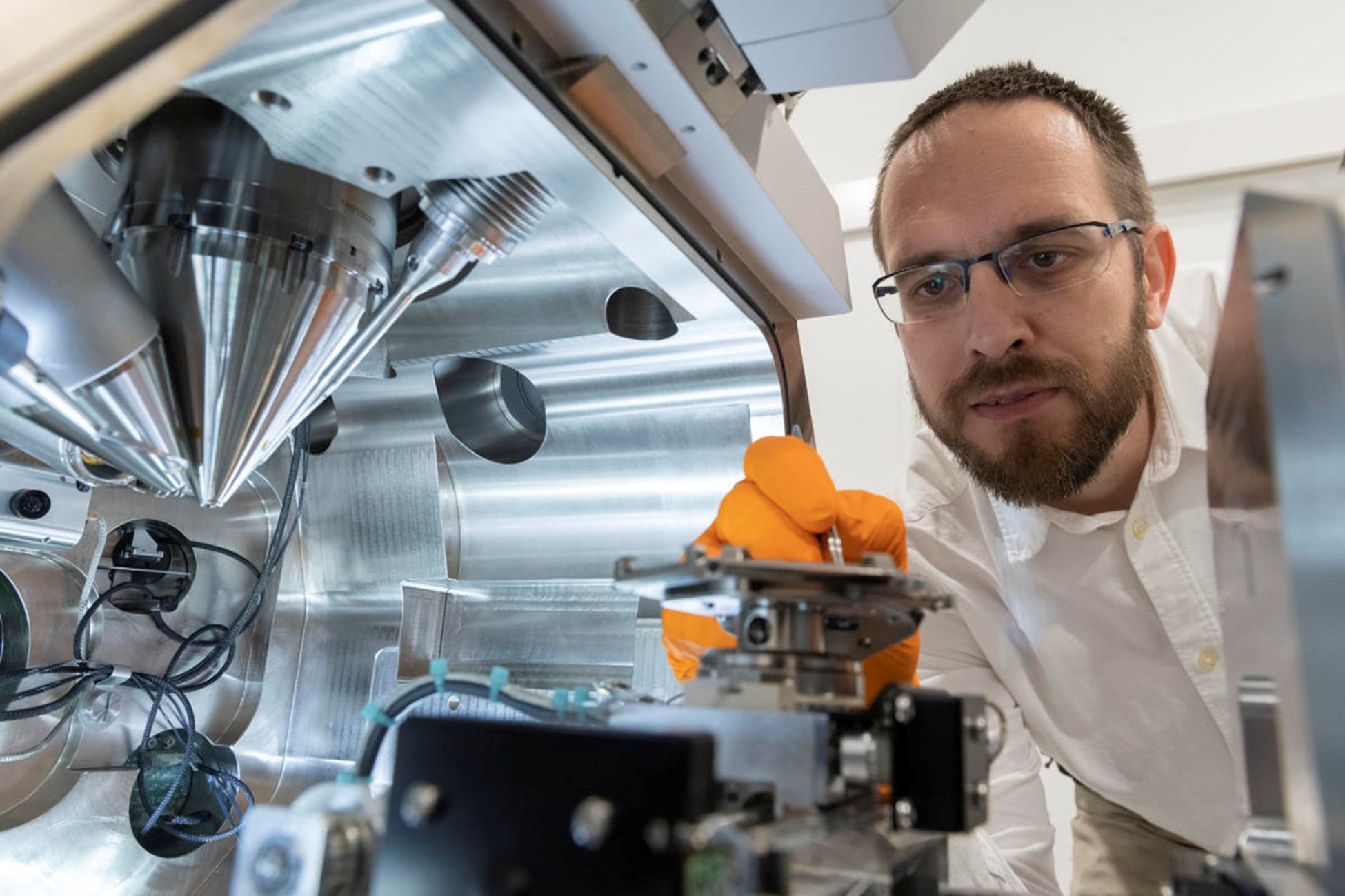
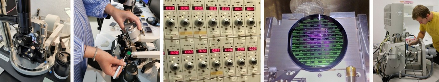
HRTEM/FIB training in MFA Budapest
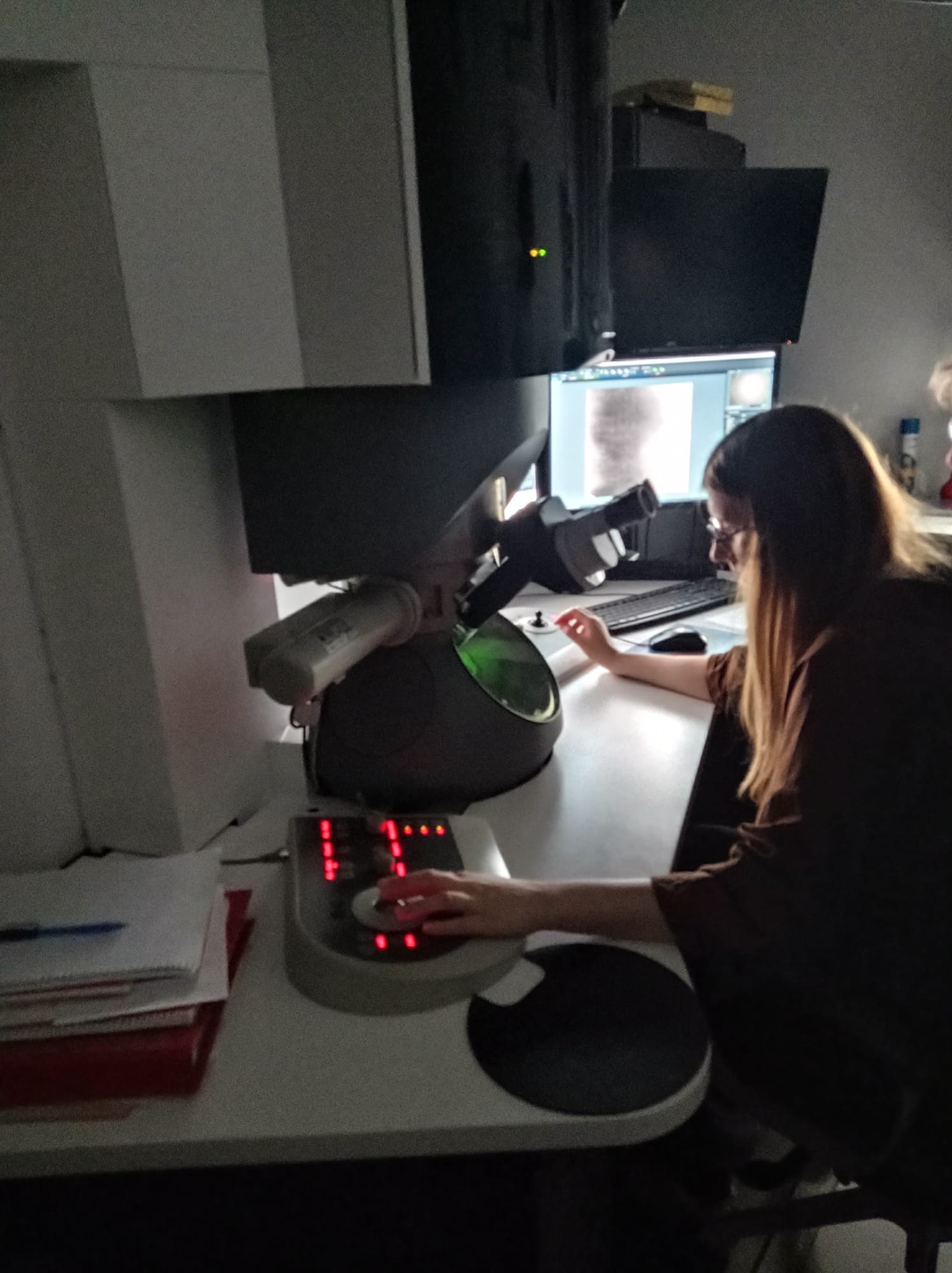
As a part of the short-term interinstitutional mobilities we have organised the training dedicated to the high-resolution transmission electron microscopy imaging and lamellae preparation by conventional techniques and focused-ion beam method. The training was held in Budapest at the Centre for Energy Research MFA and led by Dr Ildikó Cora and attended by the PhD…
-
Opportunity for short-term mobilities for V4 (U)WBG experts
Partnered institutions:Institute of Electrical Engineering, Slovak Academy of Sciences (Bratislava, Slovakia)Specialises in epitaxial growth of Ga2O3, III-N, and III-V materials, thin-film deposition techniques (ALD, PVD, PLD), device processing technology, materials diagnostics and device electrical testing Łukasiewicz Institute of Microelectronics and Photonics (Warsaw, Poland)Specialies in thin-film deposition techniques of oxides (NiO, ZnO, AZO,..), device processing, and…
-
Workshop on (U)WBG semiconductor materials and devices
A dedicated workshop will take place on April 28th-29th, 2025 in Budapest (Hungary), to share and disseminate the key scientific results obtained during the project, provide tutorial lectures, and discuss future directions. The event will serve as a platform for strengthening the existing collaborations within the established network of researchers from the V4 countries, all…
-
HRTEM/FIB training in Budapest
From April 24th to April 30th, 2025, a specialized training will be held in Centre for Energy Research, MFA, Budapest, offering participants an excellent opportunity to explore advanced methodologies in high-resolution transmission electron microscopy (HRTEM), focused ion beam (FIB) sample preparation, and related analytical techniques. Led by experienced MFA colleagues, this training will provide valuable…
-
Opportunity for short-term mobilities for V4 (U)WBG experts
Partnered institutions:Institute of Electrical Engineering, Slovak Academy of Sciences (Bratislava, Slovakia)Specialises in epitaxial growth of Ga2O3, III-N, and III-V materials, thin-film deposition techniques (ALD, PVD, PLD), device processing technology, materials diagnostics and device electrical testing Łukasiewicz Institute of Microelectronics and Photonics (Warsaw, Poland)Specialies in thin-film deposition techniques of oxides (NiO, ZnO, AZO,..), device processing, and…
-
Opportunity for short-term mobilities for V4 (U)WBG experts
Partnered institutions:Institute of Electrical Engineering, Slovak Academy of Sciences (Bratislava, Slovakia)Specialises in epitaxial growth of Ga2O3, III-N, and III-V materials, thin-film deposition techniques (ALD, PVD, PLD), device processing technology, materials diagnostics and device electrical testing Łukasiewicz Institute of Microelectronics and Photonics (Warsaw, Poland)Specialies in thin-film deposition techniques of oxides (NiO, ZnO, AZO,..), device processing, and…