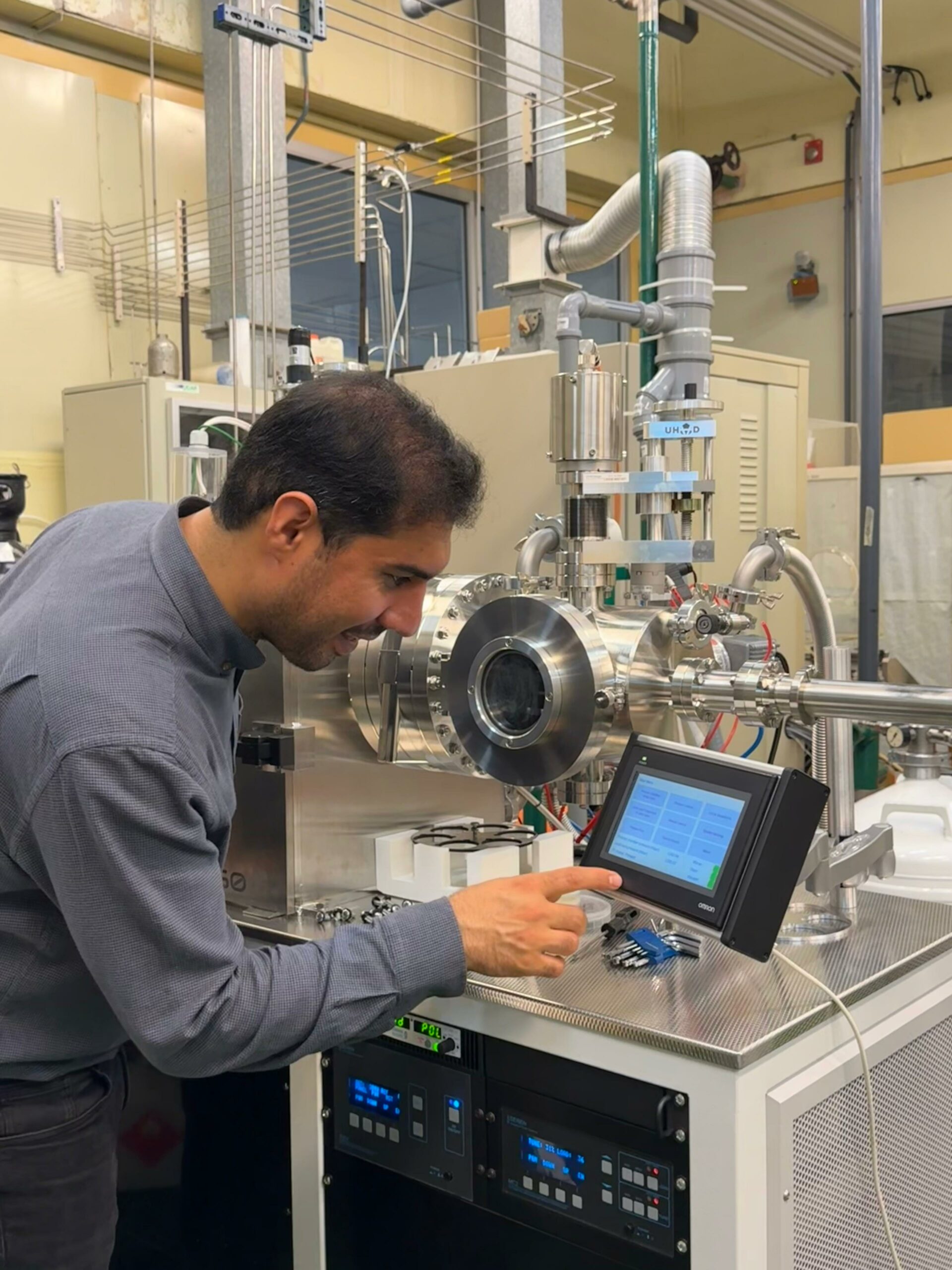
Mr Javad Keshtkar, a PhD student at the IEE SAS, has visited the Institute of Microelectronics and Photonics of Łukasiewicz Research Network in Warsaw to attend the training focused on the sputtering deposition of NiO and fabrication and electrical characterization of NiO-based thin film transistors (TFTs) for evaluation of the conductivity of the deposited NiO films.